
NIT Durgapur’s VLSI Design Achievement Takes Stage at SEMICON India 2026
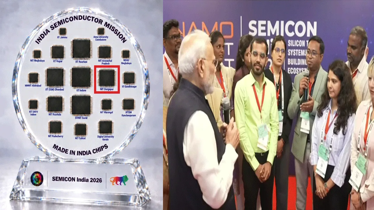
C2S Project Chip Featured in Memento Presented to Hon’ble Prime Minister Shri Narendra Modi.
National Institute of Technology Durgapur (NIT Durgapur) has achieved a significant milestone in the field of VLSI Design and semiconductor technology, with its indigenous chip developed under the Chips to Startup (C2S) Programme being featured in a special memento presented to the Hon’ble Prime Minister of India, Shri Narendra Modi, during the inaugural session of SEMICON India 2026.
At SEMICON India 2025, Hon’ble Minister of Electronics & Information Technology Shri Ashwini Vaishnaw presented the first Made-in-India chip to Hon’ble Prime Minister Shri Narendra Modi, where NIT Durgapur’s chip design, C2S0029, was proudly featured. The Department of Electronics and Communication Engineering at NIT Durgapur also successfully taped out a real chip titled “Asynchronous FIFO for Forest Event Monitoring” under the Chips to Startup (C2S) Programme of the Ministry of Electronics and Information Technology (MeitY).
Continuing this remarkable journey, the fifth edition of SEMICON India is being held from 17–19 September 2026 at Yashobhoomi (India International Convention and Expo Centre), Dwarka, New Delhi. The event brings together leading semiconductor companies, researchers, academia, startups and technology professionals from India and across the world.
The memento presented to the Hon’ble Prime Minister featured NIT Durgapur’s C2S chip, C2S0130, highlighting the institute’s contribution to indigenous VLSI and chip-design development under the C2S programme.
Congratulating the C2S project team on this significant achievement, Prof. Arvind Choubey, Director, NIT Durgapur, appreciated the dedication and technical contributions of the project investigators, faculty members, researchers and project personnel involved in the development of the indigenous chip. He noted that the recognition at SEMICON India 2026 is a proud moment for the Department of Electronics and Communication Engineering and
the Institute and reflects NIT Durgapur’s sustained commitment to fostering innovation, strengthening semiconductor research, and providing students and researchers with hands-on opportunities in VLSI design and chip development.
The chip C2S0130 is a 32-bit Fully Digital Baseband Modulator, designed as a high-precision hardware component for FPGA and ASIC platforms. The design performs the shaping, encoding and conversion of raw binary data into digital baseband signals through a fully digital architecture.
As part of the SEMICON India 2026 inauguration programme, Mr. Suman Kalyan Porel, project personnel associated with the NIT Durgapur C2S project, had the opportunity to interact with the Hon’ble Prime Minister. The achievement reflects the efforts of the entire project team, including Mr. Subhadeep Nag and Mr. Sapnil Das Choudhury, who have been actively involved in the development and implementation of the project.
Dr. Hemanta Kumar Mondal, Chief Investigator of the C2S project at NIT Durgapur, said that the recognition marks an important milestone in the institute’s continuing efforts towards strengthening VLSI design, chip development and semiconductor skill development. He emphasized that the C2S programme provides students with valuable hands-on experience in the complete chip-design flow, from RTL design and simulation to synthesis, verification and implementation, thereby enabling them to gain practical exposure to industry-relevant VLSI design methodologies. He further highlighted that such hands-on opportunities are instrumental in motivating students to pursue advanced research and careers in VLSI and semiconductor technologies.
Dr. Aniruddha Chandra, Co-Chief Investigator of the project, emphasised the importance of conceptual validation and systematic design methodology in successful chip development. He highlighted that the C2S initiative provides an opportunity for students and researchers to validate their theoretical concepts through actual hardware implementation, thereby establishing a strong connection between conceptual design, functional verification and
physical realisation. Such an approach strengthens the understanding of VLSI design principles and encourages innovation in indigenous chip development.
Prof. Rowdra Ghatak, Head of the Department of Electronics and Communication Engineering, said that it is a proud moment for the Department as well as the Institute in achieving this recognition. On behalf of the Department, we thank the Honourable Director for the continued support.
The achievement is particularly significant in the context of India Semiconductor Mission (ISM) 2.0, which places strong emphasis on strengthening semiconductor design, research, manufacturing, innovation and talent development. NIT Durgapur continues to contribute to these national objectives through its academic programmes, VLSI research activities, EDA infrastructure and participation in chip-design and tape-out initiatives.
The institute is actively working towards providing Lab-to-Fab exposure to students and researchers, enabling them to translate VLSI design concepts into fabrication-ready chip designs. Such initiatives are helping create a strong talent pipeline of engineers and researchers equipped with practical skills in ASIC, FPGA, VLSI design, verification and semiconductor technologies.
The presence of NIT Durgapur’s indigenous chip in the memento presented during SEMICON India 2026 is, therefore, a notable recognition of the institute’s contribution to India’s growing VLSI design and semiconductor ecosystem.





Recent News

Most Viewed
Lifestyle
Lifestyle
Lifestyle

Culture
Entertainment